Few industrial endeavors define the modern geopolitical era quite like the race for semiconductor supremacy. From artificial intelligence supercomputers and 5G telecommunication networks to electric drivetrains, modern fighter aircraft, and industrial robotics, microchips constitute the bedrock of national sovereignty and economic security.
Over the past five years, cascading global crises—the pandemic automotive chip freeze, rising tensions across the Taiwan Strait, and aggressive trade restrictions—have transformed semiconductor policy from a matter of corporate supply-chain logistics into a core pillar of national defence. In response, India has launched one of the most ambitious industrial programs in its history: the India Semiconductor Mission (ISM), backed by state and central fiscal incentive packages.
Yet amid the euphoria of groundbreakings and multi-billion-dollar headline announcements, a fundamental strategic question must be addressed with rigorous analytical clarity:
Can India become completely self-sufficient in semiconductors? The realistic answer is straightforward: Complete domestic self-sufficiency is virtually impossible—and economically unnecessary. A pragmatic, achievable objective is to construct a deeply resilient semiconductor ecosystem while securing indispensable, globally vital positions in selected stages of the supply chain.
Understanding what it takes to realize this ambition requires deconstructing the entire semiconductor manufacturing stack, assessing India’s true baseline today, confronting its formidable structural barriers, and embracing the philosophy of strategic specialization.
SECTION 1 — What Does a Semiconductor Supply Chain Actually Include?
Public discourse often reduces semiconductors to a single phrase: "making chips." In reality, the semiconductor supply chain is arguably the most complex, capital-intensive, and geographically dispersed manufacturing apparatus ever devised by humankind. A single finished microprocessor crosses international borders dozens of times and integrates technologies governed by specialized monopolies across ten distinct stages:
[ 1. Raw Materials ] (Quartzite, Silicon, Critical Ores)
         │
         ▼
[ 2. Specialty Chemicals & Electronic Gases ] (Ultra-pure HF, Silane, Ar)
         │
         ▼
[ 3. Wafer Manufacturing ] (Electronic-Grade Silicon Ingot Pulling, 300mm Disks)
         │
         ▼
[ 4. Chip Design & Electronic Design Automation (EDA) ] (Synopsys, Cadence, ARM, RISC-V)
         │
         ▼
[ 5. Semiconductor Capital Equipment ] (Photolithography / ASML, Etch / Lam, Deposition / Applied Materials)
         │
         ▼
[ 6. Front-End Wafer Fabrication (Foundry) ] (TSMC, PSMC, Intel, Samsung Cleanrooms)
         │
         ▼
[ 7. Assembly, Testing & Packaging (OSAT / ATMP) ] (Dicing, Wire Bonding, Epoxy Mold)
         │
         ▼
[ 8. Advanced Packaging & Heterogeneous Integration ] (2.5D/3D Chiplets, CoWoS, High-Density Substrates)
         │
         ▼
[ 9. Discrete Semiconductor Components ] (Power Transistors, Passives, Interposers)
         │
         ▼
[ 10. Downstream Electronics System Design & Manufacturing (ESDM) ] (SMT Lines, PCBs, Finished Devices)- 1. Raw Materials: The foundation starts with metallurgical-grade silicon extracted from quartzite rock, along with critical minerals including gallium, germanium, rare-earth dopants, copper, tantalum, and gold.
- 2. Specialty Chemicals and Gases: Chips require thousands of liters of electronic-grade specialty chemicals purified to 'parts-per-trillion' tolerances—such as electronic-grade hydrofluoric acid (e-HF), ultra-pure hydrogen peroxide, photoresists, silane, nitrogen trifluoride, and carrier argon.
- 3. Wafer Manufacturing: Polysilicon is melted and grown into colossal single-crystal monocrystalline ingots via the Czochralski process, which are then sliced into mirror-polished 200mm or 300mm silicon wafers with atomic-level planar flatness.
- 4. Chip Design (Fabless): Architectural innovation powered by Electronic Design Automation (EDA) software suites (Synopsys, Cadence, Siemens EDA) and Instruction Set Architectures (x86, ARM, RISC-V), translating logical algorithms into billions of transistor layout coordinates.
- 5. Semiconductor Capital Equipment: The high-precision machinery required to manipulate matter at the nanometer scale—Extreme Ultraviolet (EUV) and Deep Ultraviolet (DUV) lithography scanners (ASML), atomic layer deposition tools (Applied Materials), plasma etch systems (Lam Research), and ion implanters.
- 6. Front-End Wafer Fabrication: The pure cleanroom manufacturing process where bare silicon wafers undergo hundreds of sequential photolithography, deposition, etching, chemical mechanical planarization (CMP), and ion doping cycles to form active integrated circuits.
- 7. Assembly, Testing, and Packaging (ATMP / OSAT): Once processed, wafers are thinned, diced into individual silicon dies, mounted onto lead frames or substrates, wire-bonded or solder-bumped, encapsulated in protective epoxy resin, and rigorously stress-tested.
- 8. Advanced Packaging: Cutting-edge heterogeneous integration techniques—such as 2.5D/3D die stacking, silicon interposers, and Wafer-Level Packaging (WLP)—allowing multiple specialized dies (e.g., GPU compute dies bonded directly alongside High-Bandwidth Memory dies) to function as a unified high-speed system.
- 9. Discrete Semiconductor Components: Supporting power management ICs (PMICs), silicon carbide (SiC) and gallium nitride (GaN) power transistors, diodes, and RF modules that regulate voltage and high-frequency communication in end products.
- 10. Electronics System Design and Manufacturing (ESDM): The final stage where packaged chips, surface-mount passives, connectors, and printed circuit boards (PCBs) are populated and integrated into commercial smartphones, automotive ECUs, avionics, servers, and consumer electronics.
SECTION 2 — Where Does India Stand Today?
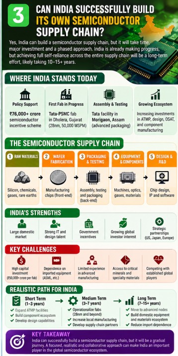
To chart a credible future path, one must differentiate between where India currently leads and where its ecosystem is still embryonic. India's semiconductor landscape in 2026 is characterized by world-class software and architectural design talent operating alongside nascent physical hardware fabrication.
| Supply Chain Stage | India's Current Standing (2026) | Strategic Maturity Level |
| Chip Design & EDA Engineering | Global powerhouse: ~20% of world's chip designers; R&D hubs for Qualcomm, Intel, NVIDIA | High / Globally Dominant |
| Electronics Assembly (ESDM) | Massive scale in smartphones and consumer appliances (Foxconn, Pegatron, Dixon Technologies) | High & Rapidly Expanding |
| Domestic Electronics Market | One of the fastest-growing consumption markets for 5G, automotive, and power devices | High & Expanding |
| OSAT / ATMP Packaging | Major greenfield plants under active construction (Micron Sanand, Tata Jagiroad, CG Semi) | Emerging / Inflection Point |
| Commercial Front-End Fab | First commercial 300mm fab underway at Dholera; historical facilities limited to legacy R&D (SCL) | Early / Construction Phase |
| Specialty Gases & Chemicals | Strong bulk chemical industry, but electronic parts-per-trillion purification remains imported | Low to Moderate |
| Capital Equipment & Lithography | Complete foreign reliance on ASML, Applied Materials, Lam, Tokyo Electron | Negligible (Heavy Import Reliance) |
| Wafer Ingot Slicing (Silicon Substrates) | Virtually zero domestic commercial 300mm electronic-grade wafer pulling | Negligible (Import Dependent) |
India's Core Foundational Strengths
India’s greatest immediate asset is its intellectual capital. Nearly every leading multinational semiconductor company—including Qualcomm, Texas Instruments, Intel, NVIDIA, AMD, MediaTek, and NXP—operates massive engineering centers across Bengaluru, Hyderabad, Noida, and Pune. Tens of thousands of Indian engineers contribute daily to tape-outs of complex microprocessors, AI accelerators, and RF transceivers. Furthermore, India’s domestic consumption market provides natural demand absorption for consumer goods, electric mobility, and telecommunications equipment.
The Developing Infrastructure Landscape
Until recently, India’s physical manufacturing capabilities were confined to niche government facilities like the Semi-Conductor Laboratory (SCL) in Mohali, primarily servicing defence and space requirements on older 180nm processes. Today, the country is executing a coordinated transition toward commercial-scale physical infrastructure across three pillars:
- Commercial Front-End Fabs: Establishing high-volume 300mm wafer fabrication capacity to anchor the domestic hardware ecosystem.
- OSAT and ATMP Hubs: Rapidly deploying assembly and packaging units that require lower capital expenditure, yield faster turnaround times, and generate immediate industrial employment.
- Design-Linked Incentives (DLI): Supporting indigenous fabless chip startups to retain domestic intellectual property rather than merely functioning as offshore design service hubs.
SECTION 3 — India's Semiconductor Manufacturing Push
India's ongoing semiconductor drive is catalyzed by the central government's ₹76,000 crore (~$10 billion) incentive umbrella under the India Semiconductor Mission (ISM), complemented by 20% to 25% matching capital subsidies from state governments. Rather than pursuing speculative projects, the current push is anchored by blue-chip domestic conglomerates partnering with veteran global technology providers.
Key Announced Projects and Industrial Anchors
- Tata Electronics and PSMC Fab (Dholera, Gujarat): Tata Electronics has partnered with Taiwan’s Powerchip Semiconductor Manufacturing Corporation (PSMC) to construct India’s first commercial mega-fab in Dholera Special Investment Region. With an announced projected investment of approximately ₹91,000 crore (~$11 billion), the facility targets a capacity of up to 50,000 wafer starts per month (WSPM). Critically, it focuses on mature nodes—28nm, 40nm, 55nm, and 90nm—serving automotive microcontrollers, power management ICs, industrial automation, and display drivers.
- Tata Semiconductor Assembly and Test (Jagiroad, Assam): In a landmark expansion for northeastern industrial development, Tata Electronics is establishing an advanced semiconductor packaging facility in Jagiroad, Assam, with an announced investment outlay of approximately ₹27,000 crore (~$3.2 billion). The facility will focus on wire-bond, flip-chip, and integrated packaging for automotive, communications, and consumer applications, with projected capacity exceeding 48 million chips daily.
- Micron Technology ATMP Facility (Sanand, Gujarat): Global memory giant Micron has committed to a phased semiconductor assembly, test, marking, and packaging facility in Sanand, Gujarat, with an announced combined investment of up to $2.75 billion (comprising Micron’s equity and combined central/state government incentives). The facility packages dynamic random-access memory (DRAM) and NAND flash modules for domestic systems and global export.
- CG Semi and Renesas JV (Sanand, Gujarat): Murugappa Group’s CG Power, partnering with Japan’s Renesas Electronics and Thailand’s Stars Microelectronics, is establishing an outsourced assembly and test facility with an announced investment of approximately ₹7,600 crore, focusing on specialized automotive and power modules.
- Kaynes Semicon (Sanand, Gujarat): Kaynes Technology’s semiconductor division is setting up an OSAT facility with an announced investment of approximately ₹3,300 crore to produce multi-chip modules and power devices.
Together, these announced investments represent over ₹1.5 lakh crore (~$18 billion) in committed capital expenditure across front-end fabrication and back-end packaging.
SECTION 4 — India's Strategic Strengths
Building a competitive semiconductor ecosystem is impossible in an economic vacuum. India possesses distinct, structural advantages that make its current attempt substantially more viable than historical efforts in the 1980s and 2000s:
- 1. Massive Domestic Electronics Market: India is the second-largest smartphone market globally and one of the fastest-growing markets for two-wheeler and four-wheeler electric vehicles, renewable power inverters, and digital infrastructure. Domestic fab output has a built-in captive customer base.
- 2. Immense Engineering Talent Pool: India graduates hundreds of thousands of STEM engineers each year. Its deep bench of circuit design, verification, and software engineering talent provides an immediate human capital foundation.
- 3. Established IT and Chip-Design Ecosystem: Having hosted global design centers for three decades, India's engineers are thoroughly versed in cutting-edge EDA software, physical layout synthesis, and design-for-manufacture (DFM) methodologies.
- 4. Robust, Long-Term Government Incentives: The India Semiconductor Mission offers a transparent 50% central fiscal capital subsidy on a pari-passu basis, paired with substantial state subsidies, streamlined environmental clearances, and designated industrial corridors.
- 5. Geopolitical Alignment & 'China+1' Friend-Shoring: Global democratic nations and technology conglomerates are actively seeking to diversify their manufacturing footprints away from concentrated choke points in Greater China. India offers scale, democratic governance, and rule of law.
- 6. Booming Downstream Electronics Manufacturing (ESDM): Enabled by schemes like the Production-Linked Incentive (PLI) for Large Scale Electronics Manufacturing, companies like Apple (via Foxconn, Pegatron, and Tata) now manufacture significant shares of flagship smartphones in India, closing the loop between chip packaging and device assembly.
- 7. Strategic International Partnerships: Bilateral semiconductor memorandums of understanding with the United States, Japan, the European Union, and Singapore, alongside engagement in the Minerals Security Partnership (MSP), facilitate technology transfer, workforce exchange, and critical mineral sourcing.
- 8. Expanding Ancillary Industrial Base: Established domestic strengths in heavy chemical synthesis, precision steel manufacturing, and industrial gas separation provide an emerging base to develop localized tier-2 input suppliers.
SECTION 5 — India's Biggest Structural Challenges
While enthusiasm is justified, constructing semiconductor manufacturing facilities is among the most unforgiving technical undertakings in industrial history. Policymakers and industry analysts must confront the severe structural bottlenecks that can derail progress if unaddressed:
- A. Staggering Capital Requirements: A modern commercial fabrication facility requires $5 billion to $12 billion in initial capital expenditure, followed by $1 billion or more in annual reinvestment to maintain equipment and upgrade processes. Fabs depreciate rapidly; failure to run equipment at 85%+ capacity utilization leads to crippling financial burn.
- B. Deep Technology Dependence: Semiconductor manufacturing process recipes (Process Design Kits / PDKs) are closely guarded intellectual property. India currently relies entirely on foreign technology partners (such as Taiwan's PSMC) to license front-end process nodes.
- C. Imported Semiconductor Capital Equipment: Every advanced machine inside a cleanroom—from multi-million-dollar lithography steppers to atomic-layer chemical vapor deposition (CVD) chambers—must be imported from the Netherlands, the United States, or Japan. India has zero domestic manufacturing for precision cleanroom tools.
- D. Advanced Lithography Monopolies: Leading-edge fabrication is permanently bottlenecked by Dutch monopoly ASML, which builds 100% of the world's commercial Extreme Ultraviolet (EUV) lithography systems. As detailed in our analysis of global AI hardware choke points, acquiring and maintaining these systems requires astronomical capital, strict geopolitical clearance, and decades of optical expertise.
- E. Specialty Chemicals Deficit: Wafer etching and cleaning demand ultra-pure electronic-grade chemicals (hydrofluoric acid, sulfuric acid, ammonium hydroxide, photoresists) purified to parts-per-trillion purity. Standard industrial chemicals contain contaminants that destroy nanometer-scale circuitry.
- F. Semiconductor-Grade Gas Supply: Epitaxial wafer growth requires ultra-pure silane, germane, phosphine, and carrier argon. Establishing reliable domestic refining and cryogenic transport for these highly reactive, hazardous gases is a massive logistical challenge.
- G. Extreme Water and Uninterrupted Power Needs: A single commercial fab consumes 3 to 5 million gallons of Ultra-Pure Water (UPW) daily—filtered to eliminate virtually all microscopic minerals and bacteria. Furthermore, fabs require hundreds of megawatts of continuous, harmonic-free electrical power. A single microsecond voltage drop can destroy an entire production lot of wafers worth millions of dollars.
- H. Shop-Floor Cleanroom Workforce Gaps: While India has tens of thousands of software and circuit design engineers, it suffers from a severe shortage of hands-on cleanroom technicians, yield-optimization process engineers, and precision maintenance specialists who understand vacuum pumps, robotic wafer handlers, and toxic gas abatement.
- I. Lack of Deep Supplier Ecosystem Clusters: In Hsinchu (Taiwan) or Silicon Valley, hundreds of precision machine shops, quartzware fabricators, and calibration specialists operate within a 30-minute radius of fabs. In India, if a critical vacuum valve or mass flow controller fails, replacement components often have to be flown in from overseas, risking costly downtime.
- J. Fierce Global Subsidy Competition: India is not building its ecosystem in isolation. The United States ($52 billion CHIPS Act), the European Union (€43 billion European Chips Act), South Korea ($470 billion mega-cluster plan), China ($47+ billion Big Fund III), and Japan are pouring unprecedented state subsidies into their own domestic industries.
SECTION 6 — India Does NOT Need to Make Everything: The Strategic Specialization Imperative
The single most common misconception in semiconductor policy is that national security requires a country to build every single piece of the supply chain on domestic soil. In reality, no country on Earth has ever achieved total semiconductor autarky—not the United States, not Taiwan, not Japan, and not China.
The United States designs the world's most advanced microprocessors (NVIDIA, Apple, Qualcomm) and owns the premier EDA software suites (Synopsys, Cadence), but relies on Taiwan for front-end fabrication and the Netherlands for photolithography. Taiwan fabricates the world's fastest chips, but relies entirely on imported silicon wafers from Japan, chemical photoresists from Tokyo Ohka Kogyo, and lithography scanners from ASML. Japan produces indispensable photoresists and silicon wafers, but lost its leading-edge foundry crown decades ago.
The Principle of 'Strategic Specialization'
Instead of attempting an economically ruinous quest for complete autarky, India’s guiding strategy must be Strategic Specialization. Under this framework, India focuses capital, policy, and research on segments where it can rapidly establish competitive scale, while relying on trusted allied networks for hyper-specialized front-end machinery.
By mastering specific high-value segments, India can build 'Bottlenecks of Bottlenecks'—critical industrial nodes that global supply chains cannot bypass. High-potential strategic specialization domains include:
- Semiconductor Packaging (OSAT / ATMP): Assembly, test, and packaging requires one-fifth the capital expenditure of a mega-fab, creates five to ten times more direct jobs, and provides immediate supply resilience for domestic electronics assemblers.
- Fabless Chip Design & IP Ownership: Supporting domestic fabless startups through the Design-Linked Incentive (DLI) scheme allows Indian engineers to create proprietary microcontrollers for two-wheelers, smart meters, UPI terminals, and local telecommunications infrastructure.
- Power Semiconductors (SiC & GaN): Silicon Carbide (SiC) and Gallium Nitride (GaN) compound semiconductors are critical for electric vehicle inverters, high-speed rail, solar power inverters, and fast chargers. They operate on mature nodes (150mm–200mm wafers) that do not require multi-billion-dollar EUV scanners.
- Automotive and Industrial Microcontrollers (28nm to 65nm): Legacy nodes represent over 70% of global semiconductor demand by volume. Dominating mature node production insulates India's automotive and consumer durable sectors from global supply crunches.
- Specialty Gases and Byproduct Extraction: Utilizing India’s vast steel and aluminum smelting infrastructure (such as NALCO's bauxite refineries) to extract high-purity gallium and capture semiconductor-grade noble gases like neon and argon.
- Rare-Earth Permanent Magnets: Transitioning from raw monazite sand mining in Kerala and Odisha into domestic neodymium-iron-boron (NdFeB) sintered permanent magnet production, countering Chinese export restrictions.
- Semiconductor Precision Tool Components: Building precision CNC machining, quartzware fabrication, and vacuum chamber components to supply global equipment titans like Applied Materials and Lam Research.
SECTION 7 — India's Semiconductor Supply Chain Roadmap
Building an industrial ecosystem is not an overnight leap; it is a multi-generational, phased evolution. Below is a structured strategic planning roadmap outlining the realistic phases of development over the next 15 years. (Note: These represent strategic planning horizons, not guaranteed government delivery deadlines.)
| Phase Horizon | Primary Strategic Objectives | Key Focus Areas & Milestones |
| Short Term (1–3 Years: 2026–2029) | Operationalize packaging anchors & seed supplier base | • Commission Micron Sanand and Tata Jagiroad packaging plants • Commence cleanroom construction at Tata-PSMC Dholera fab • Deploy university cleanroom curriculums to train 20,000+ technicians • Attract tier-2 specialty gas and chemical suppliers to Gujarat & Assam • Expand DLI approvals for indigenous fabless startups |
| Phase Horizon | Primary Strategic Objectives | Key Focus Areas & Milestones |
| Medium Term (3–7 Years: 2029–2033) | Commercial wafer output, mature node scaling & packaging expansion | • Commercial 300mm wafer output at Dholera on 28nm/40nm/90nm nodes • Scale advanced packaging (flip-chip, 2.5D integration, SiP) • Qualify domestic chemical suppliers for electronic-grade acids • Achieve 40%+ domestic silicon sourcing for Indian smartphone/automotive assembly • Expand compound semiconductor foundries (SiC/GaN) for EV power electronics |
| Phase Horizon | Primary Strategic Objectives | Key Focus Areas & Milestones |
| Long Term (7–15+ Years: 2033–2040+) | Global niche leadership, advanced nodes & domestic tooling | • Progress toward sub-14nm FinFET manufacturing capabilities • Build domestic manufacturing for subsystem tools (vacuum pumps, inspection stages) • Establish major global market share in automotive chips & compound semiconductors • Attain strategic import resilience across critical precursor chemicals • Transform Indian fabless startups into global semiconductor IP giants |
SECTION 8 — Can India Compete With Taiwan, South Korea, and China?
Any analytical assessment must avoid nationalistic hype and objectively evaluate India's competitive positioning relative to entrenched global titans:
- Taiwan (TSMC, UMC, ASE Group): Taiwan possesses a multi-decade head start, the world's densest industrial supplier cluster, and unrivaled manufacturing yields on sub-3nm nodes. Matching TSMC's cutting-edge foundry efficiency is neither realistic nor necessary for India in the foreseeable future.
- South Korea (Samsung, SK Hynix): South Korea commands over 70% of the world's memory market (DRAM, NAND flash) and is the sole global leader alongside Micron in High-Bandwidth Memory (HBM) required for AI workloads. Competing head-to-head in commodity memory would require dozens of billions in speculative capital with razor-thin cyclical margins.
- China (SMIC, CXMT, YMTC): China has invested over $150 billion in state capital over the last decade, developing colossal domestic capacity in legacy nodes (28nm–65nm) and aggressively building indigenous tooling to withstand Western export bans. China’s manufacturing scale and speed of execution remain formidable benchmarks.
- The United States and Japan: The US leads the world in chip architecture, EDA tools, and equipment IP, while Japan dominates specialty chemicals, wafer slicing, and precision robotics.
Where India Can Build Real Competitive Advantage
India does not need to beat Taiwan at 2nm logic or displace South Korea in DRAM to become an indispensable semiconductor power. Instead, India's competitive wedge lies in:
- The Global Design Hub: Transforming its existing base of 20% of global design engineers from cost-center contractors into creators of indigenous, high-margin semiconductor intellectual property.
- High-Volume Advanced OSAT / ATMP: Becoming the premier global alternative to Southeast Asia (Malaysia, Vietnam) for back-end packaging and test operations.
- Captive End-to-End Electronics Integration: Combining chip packaging, PCB manufacturing, and final device assembly within the same domestic industrial corridors, minimizing international shipping times and tariffs.
- Specialized Compound Semiconductors & Power Chips: Capturing global market share in silicon carbide and gallium nitride devices essential for the global electric vehicle and renewable energy transition.
SECTION 9 — What India Should Prioritize: A 7-Point Strategic Roadmap
To maximize return on capital and build lasting structural resilience, India’s policymakers and industry leaders should focus on seven clear operational priorities:
[ 1. Build Packaging Scale ] ──► [ 2. Develop Domestic Materials ] ──► [ 3. Attract Tool Vendors ]
               │                                   │                                    │
               ▼                                   ▼                                    ▼
[ 4. Scale Cleanroom Workforce ] ──► [ 5. Strengthen Fabless Design ] ──► [ 6. Localize Components ]
                                                   │
                                                   ▼
[ 7. Secure Strategic Alliances ]- 1. Build Packaging Scale (OSAT / ATMP First): Prioritize fast execution on packaging plants. OSAT facilities create immediate employment, require manageable water and power footprints, and yield operational revenue within 18 to 24 months, providing immediate cash flow to seed the broader ecosystem.
- 2. Develop Semiconductor Materials and Chemicals: Extend targeted production-linked subsidies to specialty chemical synthesis plants capable of producing electronic-grade acids, high-purity hydrogen peroxide, and semiconductor gases (argon, silane, nitrogen).
- 3. Attract Global Equipment Maintenance and Tool Vendors: Incentivize capital equipment leaders (Applied Materials, Lam Research, KLA, ASML) to establish major regional refurbishment, calibration, and spare parts warehousing centers in India, ensuring local fabs do not suffer extended downtime.
- 4. Build a Skilled Cleanroom and Process Workforce: Modernize university curricula and polytechnic vocational programs. Cleanrooms require tens of thousands of specialized technicians trained in vacuum systems, chemical handling, particulate control, and statistical process monitoring.
- 5. Strengthen Indigenous Fabless Chip Design: Expand the Design-Linked Incentive (DLI) scheme with dedicated venture funding and government procurement mandates, ensuring Indian fabless startups design chips specifically optimized for domestic infrastructure (smart energy meters, EV drivetrains, defence communication).
- 6. Localize Subsystem and Component Suppliers: Encourage precision engineering and CNC machining manufacturers to produce quartzware, vacuum flanges, ceramic heaters, and fluid-handling subsystems required by fab operators.
- 7. Create Long-Term Strategic International Partnerships: Cement multi-lateral joint ventures under the Quad and the Minerals Security Partnership (MSP) to secure reliable supplies of refined gallium, silicon carbide boules, and rare-earth magnets from friendly nations.
SECTION 10 — The Real Meaning of Semiconductor Self-Reliance
The modern semiconductor debate often suffers from binary thinking: either complete autarky or total vulnerability. This is a false dichotomy.
True self-reliance does not mean manufacturing every single diode, gas molecule, and optical mirror inside domestic borders. In an interconnected global economy, self-reliance means having enough domestic operational capability, diversified vendor relationships, and strategic reserve capacity that an external crisis or foreign blockade cannot paralyze the nation's industry.
Consider energy security: India imports the majority of its crude oil, yet maintains strategic oil reserves, domestic refining capacity, and diversified import contracts to ensure supply stability. The same principle applies to microelectronics. By controlling mature-node fabrication for foundational infrastructure, mastering packaging, nurturing world-class design houses, and securing strategic mineral stockpiles, India insulates its economic sovereignty from overseas geopolitical turmoil.
Conclusion: An Indispensable Link in the Global Chain
Returning to our core opening inquiry:
"Can India successfully build its own semiconductor supply chain?"
Yes, India can successfully build a semiconductor supply chain—but not overnight, and not by trying to manufacture everything itself. The journey requires measured realism, consistent fiscal commitment across political cycles, and disciplined execution.
India's pragmatic, achievable destination is not an isolated semiconductor island, but a pivotal global node: a world-class semiconductor packaging and assembly capital, an electronics manufacturing base of massive scale, an indigenous chip-design powerhouse, and a vital producer of specialized compound semiconductors and materials.
India does not need to own every link in the semiconductor chain. It needs to make enough links indispensable.